|
Minimus32

Intro
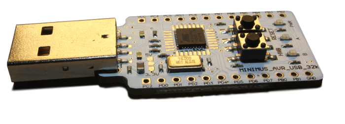
The reason for creating this page is very simple.
The creators of the Minimus32 seemed very unwilling to publish the schematics for the otherwise excellent Minimus32 (development board)
And if I were to discover the function of the 3.3V/5V solder jumper and other nice to know stuff I might as well share my results with you.
And before the DIY folks out there starts to copy the Minimus32, please take a look at the prices you can get one for...
They are cheap!
Links
Schematic and other information
Please note that this information just represents my best guess of how the board is constructed.
It is for instance difficult to measure component values without removing them.
And even harder to determine non passive components like the two unknown components that is probably protecting the USB port.
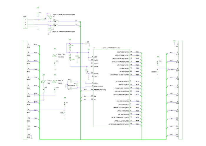
Schematic
NOTES:
- F1 might just a well be a inductor as a fuse, I just hope its a fuse (to prevent damage to your UBS port).
- Z1 and Z2 is some sort of non resistive component, probably some sort of protection from ESD damage to the USB transceivers.
- I haven't seen the trace connecting Vcc to 5V and therefor can't say for sure if Vcc is connected directly til AVcc, but is would make a lot of sense.
(The trace would probably be hidden below the MCU)

As a gschem schematics file
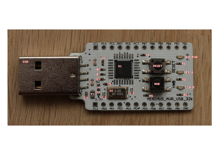
Silk screen

Bill Of Materials
NOTE: Only resistors have actually been measured.
| C1 | 1 µF is suggested by the data sheet for the decoupling/output cap for the internal 3.3V regulator. |
| C2 | 15 pF? Data sheet suggests 12-22pF for the crystal caps. |
| C3 | 15 pF? Data sheet suggests 12-22pF for the crystal caps. |
| C4 | "Bulk" input decoupling cap, 1 µF perhaps (to keep the number of different parts low).
Could also be some sort of ESD protection but I don't think so. |
| C5 | MCU decoupling cap, perhaps 100nF. |
| C6 | MCU decoupling cap, perhaps 100nF. |
| F1 | I hope it is a fuse, a fast acting 100mA one would be nice... Could also be an inductor or perhaps some entirely different component? |
| HWB | A push button. |
| J1 | A solder jumper, seems to be hardwired ON by a PCB trace.
I have seen photos of earlier(?) PCBs witch were soldered. |
| J2 | A solder jumper.
CAUTION: Don't just apply solder here without knowing exactly what you are doing! |
| LED_A | A red LED. |
| LED_B | A blue LED. |
| LED_PWR | A green LED. |
| R1 | 1k Ohm series resistor for the LED. |
| R2 | 1k Ohm series resistor for the LED. |
| R3 | 1k Ohm series resistor for the LED. |
| R4 | 47k Ohm pull up for the switch.
Measured to ~46.5k Ohm but I assume that its just a low precision resistor. |
| R5 | 47k Ohm pull up for the switch.
Measured to ~46.5k Ohm but I assume that its just a low precision resistor. |
| R6 | 22 Ohm resistor. |
| R7 | 22 Ohm resistor. |
| RESET | A push button. |
| U1 | ATMEGA32U2 MCU. |
| U2 | 16 MHz crystal |
| Z1 | Non resistive component, probably ESD protection, maybe it's a zener diode? |
| Z2 | Non resistive component, probably ESD protection, maybe it's a zener diode? |
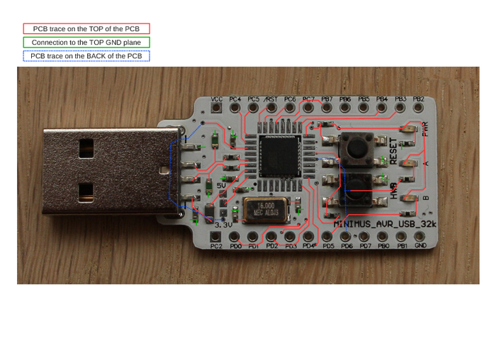
PCB traces
I have traced some of the more interesting PCB traces on the image below.

3.3V power
The ATMEGA32U2 has a 3.3V regulator build in for supplying power for the USB transceivers.
This regulator can also be used to power the chip and peripherals.
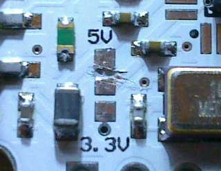
In order to switch to 3.3V power you need to cut the PCB trace between the 5V and the centre pad.
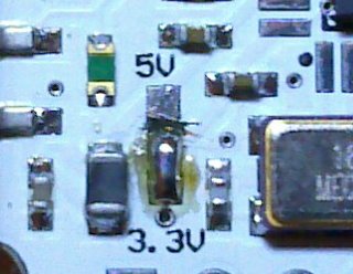
After this you just bridge the centre to 3.3V gab with solder.
The solder mask may/will cause you problems bridging the gab, a thin strand of copper wire can be used to help the solder forming the bridge.
CAUTION: Always make sure that you don't short 5V to 3.3V with the solder bridge, doing so will probably ruin the ATMEGA32U2.
Available current
The data sheet seems to be somewhat vague when it comes to specifying the maximum current draw allowed for the regulator.
- The min,avg and max output voltage for the regulator are specified at I=100mA with a supply voltage of 4V.
- If the 100mA is a thermal limit the max. current will have dropped to ~63mA @ 5V which is a more likely supply voltage.
- Chris McClelland gave me a tip: The AT90USB162 data sheet claims that at least 50mA is available for peripherals.
- The ATMEGA32U2 data sheet contains voltage vs. input voltage graphs with a 75 Ohm load on the 3.3V line ~44mA.
When looking at the figures please remember to take into account that the USB transceivers, the MCU it self and not the least the Minimus32 LEDs also draws current.
Images
 
|
